(China (Mainland))


Product Summary
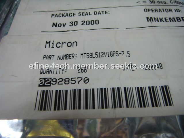
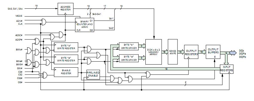
The MT58L512V18PS-7.5 is an 8Mb SYNCBURST SRAM. The device employs high-speed, low-power CMOS designs that are fabricated using an advanced CMOS process. The MT58L512V18PS-7.5 integrates a 512K x 18 SRAM core with advanced synchronous peripheral circuitry and a 2-bit burst counter. All synchronous inputs pass through registers controlled by a positive-edge-triggered single-clock input (CLK).
Parametrics
MT58L512V18PS-7.5 absolute maximum ratings: (1)Voltage on VDD Supply: Relative to VSS: -0.5V to +4.6V; (2)Voltage on VDDQ Supply: Relative to VSS: -0.5V to +4.6V; (3)VIN (DQx): -0.5V to VDDQ + 0.5V; (4)VIN (inputs): -0.5V to VDD + 0.5V; (5)Storage Temperature (plastic): -55°C to +150°C; (6)Storage Temperature (FBGA): -55°C to +125°C; (7)Junction Temperature: +150°C; (8)Short Circuit Output Current: 100mA.
Features
MT58L512V18PS-7.5 features: (1)Fast clock and OE# access times; (2)Single +3.3V +0.3V/-0.165V power supply (VDD); (3)Separate +3.3V or +2.5V isolated output buffer supply (VDDQ); (4)SNOOZE MODE for reduced-power standby; (5)Single-cycle deselect (Pentium? BSRAM-compatible); (6)Common data inputs and data outputs; (7)Individual BYTE WRITE control and GLOBAL WRITE; (8)Three chip enables for simple depth expansion and address pipelining; (9)Clock-controlled and registered addresses, data I/Os and control signals; (10)Internally self-timed WRITE cycle; (11)Burst control (interleaved or linear burst); (12)Automatic power-down for portable applications; (13)100-pin TQFP package; (14)165-pin FBGA package; (15)Low capacitive bus loading; (16)x18, x32, and x36 versions available.
Diagrams
 |
 MT58L128L18D |
Other |
|
Data Sheet |
Negotiable |
|
||||
|
MT58L128L18F, |
Other |
|
Data Sheet |
Negotiable |
|
||||
|
MT58L128L32D1 |
Other |
|
Data Sheet |
Negotiable |
|
||||
|
MT58L128L36D1 |
Other |
|
Data Sheet |
Negotiable |
|
||||
|
MT58L1MY18D |
Other |
|
Data Sheet |
Negotiable |
|
||||
|
MT58L256L18D1 |
Other |
|
Data Sheet |
Negotiable |
|
||||