(China (Mainland))

Product Summary
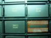
The MT47H32M16BN-3:D is a Mobile-DDR SDRAM.The MT47H32M16BN-3:D uses a double data rate architecture to achieve high-speed operation. The MT47H32M16BN-3:D with anin terface designed to transfer two data words per clock cycle at the I/O balls. A single read or write access for the DDR2 SDRAM effectively consists of a single 4n-bit-wide, oneclock-cycle data transfer at the internal DRAM core and four corresponding n-bit-wide, one-half-clock-cycle data transfers at the I/O balls. Read and write accesses to the DDR2 SDRAM are burst-oriented; accesses start at a selected location and continue for a programmed number of locations in a programmed sequence. Accesses begin with the registration of an ACTIVATE command, which is then followed by a READ or WRITE command. The address bits registered coincident with the ACTIVATE command are used to select the bank and row to be accessed. The address bits registered coincident with the READ or WRITE command are used to select the bank and the starting column location for the burst access.
Parametrics
MT47H32M16BN-3:D absolute maximum ratings: (1)VDD supply voltage relative to VSS VDD: –1.0, 2.3 V; (2)VDDQ supply voltage relative to VSSQ VDDQ: –0.5, 2.3 V; (3)VDDL supply voltage relative to VSSL VDDL: –0.5, 2.3 V; (4)Voltage on any ball relative to VSS VIN, VOUT: –0.5, 2.3 V; (5)Input leakage current; any input 0V ≤ VIN ≤ VDD;all other balls not under test = 0V II: –5, 5 μA; (6)VREF leakage current; VREF = valid VREF level IVREF: –2 2 μA.
Features
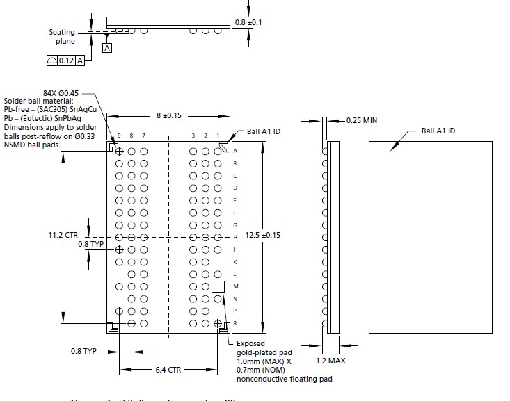
MT47H32M16BN-3:D features: (1)VDD = +1.8V ±0.1V, VDDQ = +1.8V ±0.1V; (2)JEDEC-standard 1.8V I/O (SSTL_18-compatible); (3)Differential data strobe (DQS, DQS#)option; (4)4n-bit prefetch architecture; (5)Duplicate output strobe (RDQS)option for x8; (6)DLL to align DQ and DQS transitions with CK; (7)4 internal banks for concurrent operation; (8)Programmable CAS latency (CL); (9)Posted CAS additive latency (AL); (10)WRITE latency = READ latency - 1 tCK; (11)Selectable burst lengths: 4 or 8; (12)Adjustable data-output drive strength; (13)64ms, 8192-cycle refresh; (14)On-die termination (ODT); (15)Industrial temperature (IT)option; (16)Automotive temperature (AT)option; (17)RoHS-compliant; (18)Supports JEDEC clock jitter specification.
Diagrams

| Image | Part No | Mfg | Description |  |
Pricing (USD) |
Quantity | ||||||
|---|---|---|---|---|---|---|---|---|---|---|---|---|
 |
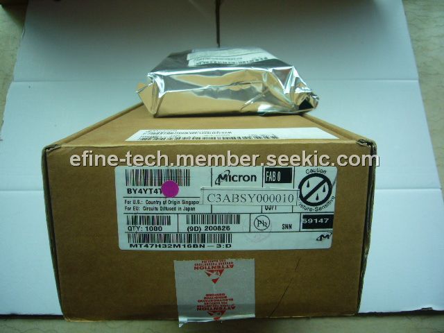
 MT47H32M16BN-3:D TR |
|
IC DDR2 SDRAM 512MBIT 3NS 84FBGA |
Data Sheet |
Negotiable |
|
||||||
| Image | Part No | Mfg | Description | |
Pricing (USD) |
Quantity | ||||||
 |
MT470 |
Other |
|
Data Sheet |
Negotiable |
|
||||||
|
MT4730NF−UBL |
Other |
|
Data Sheet |
Negotiable |
|
||||||
|
MT4730NF−WT |
Other |
|
Data Sheet |
Negotiable |
|
||||||
|
MT47H128M16PK-25E IT:C |
|
IC DDR2 SDRAM 2GB 84FBGA |
Data Sheet |
|
|
||||||
|
MT47H128M16RT-25E AIT:C |
|
IC DDR2 SDRAM 2GB 800HZ 84FBGA |
Data Sheet |
|
|
||||||
|
MT47H128M16RT-25E IT:C |
|
IC DDR2 SDRAM 2GB 800HZ 84FBGA |
Data Sheet |
|
|
||||||