(China (Mainland))


Product Summary
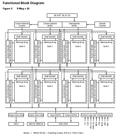
The MT49H8M36FM-5 is a 288Mb CIO Reduced Latency. The Micron® 288Mb reduced latency DRA (RLDRAM@) II is a high-speed memory device designed for high bandwidth communication data storage—telecommunications, networking, and cache applications, etc. The chip’s 8-bank architecture of MT49H8M36FM-5 is optimized for high speed and achieves a peak bandwidth of 28.8 Gb/s, using a 36-bit interface and a maximum system clock of 400 MHz. The double data rate (DDR) interface transfers two 36-, 18-, or 9-bit wide data word per clock cycle at the I/O pins. Output data is referenced to the free-running output data clock. Bank-scheduled refresh of T49H8M36FM-5 is supported with row address generated internally. A standard μBGA 144-ball package is used to enable ultra high-speed data transfer rates and a simple upgrade path from former products.
Parametrics
MT49H8M36FM-5 absolute maximum ratings: (1)Storage temperature: -55 °C, +150 °C; (2)I/O voltage: -0.3V, VDDQ + 0.3 V; (3)Voltage on VEXT supply relative to VSS: -0.3 V, +2.8 V; (4)Voltage on VDD supply relative to VSS: -0.3 V, +2.1 V; (5)Voltage on VDDQ supply relative to VSS: -0.3 V, +2.1 V; (6)Junction temperature: 110 °C.
Features
MT49H8M36FM-5 features: (1) 400 MHz DDR operation (800 Mb/s/pin data rate); (2) Organization: 8 Meg x 36, 16 Meg x 18, and 32 Meg x 9 : 8 banks; (3) Cyclic bank switching for maximum bandwidth; (4) Reduced cycle time (20ns at 400 MHz); (5) Nonmultiplexed addresses (address multiplexing option available); (6) SRAM-type interface; (7) Programmable READ latency (RL), row cycle time, and burst sequence length; (8) Balanced READ and WRITE latencies in order to optimize data bus utilization; (9) Data mask for WRITE commands; (10) Differential input clocks (CK, CK#); (11) Differential input data clocks (DKx, DKx#); (12) On-chip DLL generates CK edge-aligned data and output data clock signals; (13) Data valid signal (QVLD); (14) 32ms refresh (8K refresh for each bank; 64K refresh command must be issued in total each 32ms); (15) 144-ball μBGA package; (16) HSTL I/O (1.5V or 1.8V nominal); (17) 25Ω–60Ω matched impedance outputs; (18) 2.5V VEXT, 1.8V VDD, 1.5V or 1.8V VDDQ I/O; (19) On-die termination (ODT)RTT.
Diagrams
| Image | Part No | Mfg | Description |  |
Pricing (USD) |
Quantity | ||||||
|---|---|---|---|---|---|---|---|---|---|---|---|---|
 |
 MT49H8M36FM-5 TR |
|
IC RLDRAM 288MBIT 200MHZ 144FBGA |
Data Sheet |
Negotiable |
|
||||||
| Image | Part No | Mfg | Description | |
Pricing (USD) |
Quantity | ||||||
 |
MT49H16M16 |
Other |
|
Data Sheet |
Negotiable |
|
||||||
|
MT49H16M16FM-5 TR |
|
IC RLDRAM 256MBIT 200MHZ 144FBGA |
Data Sheet |
Negotiable |
|
||||||
|
MT49H16M18 |
Other |
|
Data Sheet |
Negotiable |
|
||||||
|
MT49H16M18BM-25:B |
|
IC RLDRAM 288MB 144UBGA |
Data Sheet |
|
|
||||||
|
MT49H16M18C |
Other |
|
Data Sheet |
Negotiable |
|
||||||
|
MT49H16M18CFM-5 IT |
|
IC RLDRAM 288MBIT 200MHZ 144FBGA |
Data Sheet |
Negotiable |
|
||||||